While exploring the STM32 Nucleo 144 board, I revisited UART: Universal Asynchronous Receiver and Transmitter. Slowly, it took me to places I wouldn’t have gone intentionally. That’s how, after a decade, I found myself once again flipping through the pages of Digital Logic Design and Computer Architecture by Morris Mano.
In circuits small, great power lies,
A thinking spark that never dies.
The microprocessor, mind in disguise.
GenAI poetic intro of a microprocessor.
Computer Systems
Knowing how computer systems work makes it easier to understand and appreciate the microprocessor. Formally, a computer is a machine that can be programmed to automatically carry out sequences of arithmetic or logical operations. A typical computer system is composed of the following core components:
- Inputs & Outputs (I/O)
- Memory
- CPU (Central Processing Unit)
The microprocessor contains the arithmetic, logic, and control circuitry required to perform the functions of a computer’s central processing unit.
In most cases, the CPU is what we refer to as a microprocessor. In some contexts, however, a microprocessor may refer to a combination of the CPU along with cache and the memory controller. But CPU is the fundamental component of a microprocessor. Today, most microprocessors are multi-core, combining multiple CPUs on a single IC (Integrated Chip).
Evolution of Microprocessor
Until the 1950s, the CPU were based on the Vacuum Tubes for execution of instructions. These tubes were massive, slow, and manually controlled, often occupying entire rooms and requiring constant manual supervision. Also they were slow to switch and prone to failure.
The invention of the transistor in 1947, revolutionized processor design. Transistors were smaller, faster, more energy-efficient, and more reliable than vacuum tubes. This pivotal shift laid the foundation for the development of integrated circuits (ICs), where multiple transistors could be embedded on a single chip.
At the heart of all this evolution lies a fundamental building block: the logic gate (like AND, OR, etc), registers, multiplexers, encoders and decoders.
The first microprocessor came in 1971, the Intel 4004 which was the first commercial 4-bit microprocessor.
Here’s a timeline of the evolution of the CPU, highlighting key milestones, innovations, and architectural shifts.
| Era | Technology | Insights |
|---|---|---|
| 1940s | Vacuum Tubes | Room-sized, manual operation |
| 1950s | Stored-program concept | Transistor begins to appear |
| 1970s | Microprocessor (VLSI) | CPU on a chip |
| 1980s | RISC vs CISC | Pipelining, early cache |
| 1990s | Superscalar | Parallel execution, multimedia |
| 2000s | Multi-core | Power efficiency, 64-bit |
| 2010s | SoC + AI Acceleration | Smartphones, ML, ARM rise |
| 2020s | Custom silicon + RISC-V | Chiplets, AI-native cores |
This transition from bulky vacuum-tube-based machines to compact silicon-based processors marks one of the most profound technological leaps in human history, one that continues to shape the trajectory of modern computing.
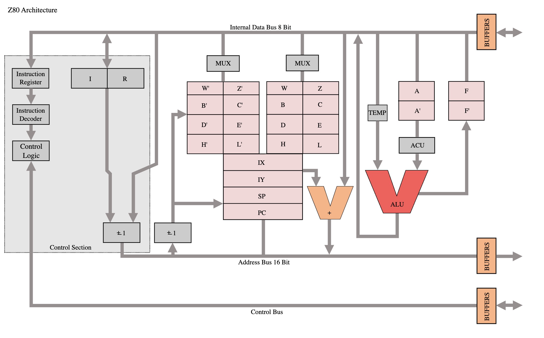
Decoding the CPU
The Central Processing Unit (CPU) is often referred to as the brain of the computer. As shown in the image above, the CPU is composed of several interconnected components that work together to perform computations. Essentially, the CPU is built from a combination of digital circuits specifically designed to fetch, decode, and execute instructions.
So what are these components? How they are made and what is the function of each component?
While a deep dive into every granular component is beyond the scope of this post, we will explore the most essential building blocks that enable the CPU to function:
- The ALU (Arithmetic Logic Unit)
- Registers (including Special Registers)
- Control Unit (Control Logic)
- Datapath
Let’s explore the components.
Arithmetic Logic Unit
The ALU is a core component of a processor responsible for carrying out arithmetic operations such as addition, subtraction, multiplication, and division, as well as logical operations like AND, OR, and XOR. Modern ALUs also support bitwise shifting and value comparisons.
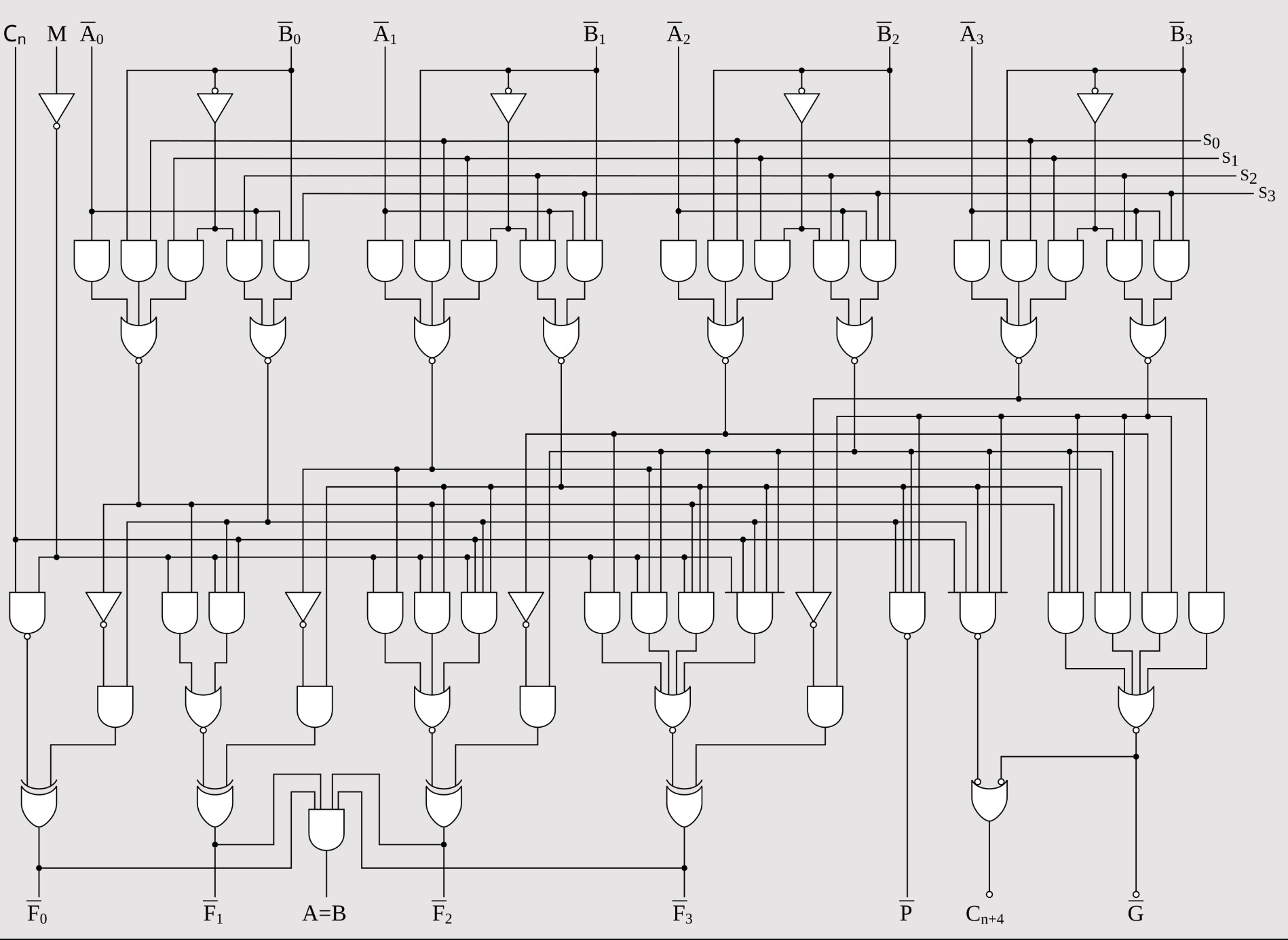
Internally, an ALU is built from basic digital components such as logic gates, adders, multiplexers, comparators, and decoders. Logic gates like AND, OR, and XOR perform boolean operations, while arithmetic operations are typically executed using adder and subtractor circuits.
Control signals derived from instruction decoding, guide the ALU in selecting the correct operation. A multiplexer chooses the final output from multiple functional paths, and comparators enable condition checking for operations like branching.
Despite its simplicity in design, the ALU performs one operation at a time but is optimized to do so very efficiently, forming the heart of computational tasks within a processor.
If you are aware of the Instruction Set Architecture which derives the development of and CPU, you can relate to the operations of the ALU. If you are willing to learn more about ISA or RISC-V, you can read my last post on the same here: RISC-V: Worth the Hype?.
Here’s the quick reference of some of the operations of the ALU that adheres to the RISC-V ISA (including the circuit they use):
| Operation | Mnemonic(s) | Circuit | RISC-V Instruction Format |
|---|---|---|---|
| Addition | ADD, ADDI |
Ripple/Carry-Lookahead Adder | R/I |
| Subtraction | SUB |
Adder + 2’s Complement | R |
| Bitwise AND | AND, ANDI |
AND Gate Array | R/I |
| Bitwise OR | OR, ORI |
OR Gate Array | R/I |
| Bitwise XOR | XOR, XORI |
XOR Gate Array | R/I |
| Set Less Than | SLT, SLTI |
Subtractor + Sign Bit Comparator | R/I |
| Shift Left Logical | SLL, SLLI |
Barrel Shifter (Left) | R/I |
| Shift Right Logical | SRL, SRLI |
Barrel Shifter (Right) | R/I |
| Equality Check | BEQ |
XOR + NOR Chain (Equality Comparator) | B |
| Not Equal Check | BNE |
Same as above | B |
| Less Than (Branch) | BLT, BLTU |
Comparator (signed/unsigned) | B |
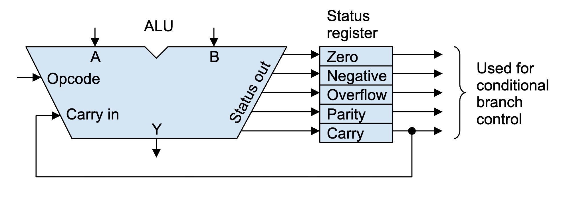
In circuit schematics, the ALU is represented by a unique symbol, typically a rectangle or trapezoid labeled “ALU” to denote its function as the core arithmetic and logic processing unit.
Registers
Registers are small, high-speed storage locations built directly into the CPU. Although registers are storage units, they are not part of the main memory but rather reside directly within the CPU. Unlike RAM, which sits further away on the memory bus, registers are right next to the ALU and control unit, allowing data to be accessed in a single clock cycle. Most CPUs come with a fixed number of general-purpose registers (like x0 to x31 in RISC-V), which are used for arithmetic, logic operations, and intermediate results.
The fewer the memory accesses, the faster the code and that’s why smart use of registers matters a lot in performance critical programs and compiler optimizations.
Register File
When we talk about registers in a CPU, we’re really talking about a structure called the register file. This is a small, fast memory block that stores all the general-purpose registers (x0 to x31 in RISC-V). Unlike RAM, the register file is built directly into the processor and is accessed in one clock cycle, it’s that fast because it has to keep up with the ALU.
The RISC-V CPUs has 32 registers all capable of holding a 32-bit number. Additionally, It also has a program counter PC register. The 32 registers labelled as x0, x1, …, x31, also has aliases assigned to them. Have a look at the RISC-V registers in the table below:
| Register | Alias | Description |
|---|---|---|
| x0 | zero |
Read only register containing 0 |
| x1 | ra |
Return address register |
| x2 | sp |
Stack Pointer |
| x3 | gb |
Global Pointer |
| x4 | tb |
Thread Pointer |
| x5-x7 | t0-t2 |
Temporary Registers |
| x8-x9 | s0-s1 |
Saved Registers |
| x10-x11 | a0-a1 |
Function arguments & returned values |
| x12-x17 | a2-a7 |
Function Arguments |
| x18-x27 | s2-s11 |
Saved registers |
| x28-x31 | t3-t6 |
Temporary registers |
Let’s get to know the special registers of the CPU.
Special Registers
Alongside the general-purpose registers, modern CPUs use a few special purpose registers to control how instructions are executed, how memory is accessed, and how the system responds to events like interrupts. These are more “behind-the-scenes” but critical to how the processor works.
Program Counter (PC)
The Program Counter keeps track of where the CPU is in the program. It holds the address of the next instruction to be executed. After each fetch, it usually increments to point to the next instruction unless a jump or branch changes it.
RISC-V uses an internal pc register to point to the current instruction. It’s automatically incremented by 4 (since RV32 instructions are 4 bytes) after each instruction. Control instructions like jal, jalr, and branches modify the PC directly.
1 | jal x0, loop # Sets PC to address labeled 'loop' (unconditional jump) |
Instruction Register (IR)
The Instruction Register temporarily holds the current instruction fetched from memory. The control unit decodes this instruction to generate signals that direct the CPU’s operations.
While RISC-V doesn’t expose the IR directly, it’s part of the fetch-decode-execute pipeline. The IR holds instructions like add, lw, beq etc., in binary form after fetch.
1 | add x5, x1, x2 # IR holds binary encoding of this instruction during decode |
Memory Address Register (MAR)
The MAR stores the memory address that the CPU wants to read from or write to. It acts as a pointer to a specific location in RAM during fetch or memory access operations.
RISC-V Internally used during load (lw) and store (sw) instructions. The effective address (base + offset) is calculated and passed through MAR to memory.
1 | lw x6, 0(x10) # MAR = x10 (base address); fetch data from memory |
Stack Pointer (SP)
The Stack Pointer tracks the top of the stack, a special region of memory used for function calls, return addresses, and local variables. It adjusts up or down as items are pushed or popped from the stack.
In RISC-V, the register x2 is reserved as the stack pointer by convention. It points to the current top of the stack, which is typically located in RAM. During function calls, the compiler or assembly code adjusts sp to allocate space for local data or save return addresses, and restores it when the function returns. This makes sp essential for managing function calls, recursion, and memory safety.
1 | addi sp, sp, -16 # Allocate 16 bytes on the stack |
Interrupt Mask (IM / Interrupt Enable Register)
This register determines which interrupts are allowed to reach the CPU. Each bit corresponds to a specific interrupt source. If the bit is set, that interrupt is enabled; if cleared, it’s masked (ignored). It allows the OS or program to selectively control what should or shouldn’t interrupt execution.
RISC-V uses the mie CSR (Machine Interrupt Enable) to enable or disable machine-level interrupts like software, timer, or external events.
1 | li t0, 0x888 # Enable MSIE, MTIE, MEIE (bits 3, 7, 11) |
Control and Status Registers (CSRs)
CSRs deal with the state of the processor itself. These special-purpose registers are crucial for things like handling interrupts, switching privilege levels, and keeping track of exceptions. You won’t see them much in simple user programs, but they’re at the heart of how an OS or trap handler talks to the hardware.
In RISC-V, CSRs are accessed using special instructions like csrrw, csrrs, and csrrc, which allow reading, writing, and modifying individual bits in these registers.
Flag Register (Status Register / Condition Code Register)
The Flag Register holds bits that reflect the outcome of operations such as:
- Zero (Z): Result was zero
- Carry (C): Result caused a carry out
- Overflow (V): Arithmetic overflow occurred
- Negative (N): Result was negative
These flags help guide conditional instructions like jumps and branches. RISC-V does not use a dedicated flag register. Instead, it uses explicit comparison instructions (beq, bne, blt, bge, etc.) to evaluate conditions directly in hardware, without relying on a status register.
This simplifies the instruction set and makes pipelines easier to implement.
1 | sub x5, x1, x2 # Perform subtraction |
Control Unit
The Control Unit (CU) is a core component of the CPU that coordinates how data moves inside the processor and how each operation is carried out. It reads the current instruction from the Instruction Register, decodes it, and generates the control signals that tell all other parts of the CPU what to do, like which registers to read, which ALU operation to perform, and when to write back results.
RISC-V, being a Reduced Instruction Set Computer (RISC) architecture, keeps its control unit simple and efficient. The instructions are fixed-width and regularly formatted (32 bits in RV32I), making decoding easier and faster.
The control unit in RISC-V performs:
- Instruction decoding
- Generating control signals (e.g. ALU operation, memory access, register write enable)
- Managing pipeline control (in pipelined implementations)
- Interacting with the program counter (PC) for branching and jumping
The control unit in a RISC-V CPU is built using a few essential hardware blocks. It starts with an opcode decoder that splits the instruction into meaningful chunks like opcode, funct3, and funct7. These values are then passed through a control signal generator, which is just a bunch of combinational logic that decides what needs to happen, like which registers to read, what operation the ALU should perform, whether to access memory, or if it’s time to branch.
In RISC-V, every instruction is 32 bits wide, and those bits are broken into specific fields. Among them, funct3 and funct7 are used for further decoding the operation when multiple instructions share the same opcode.
1 | # example: add x5, x1, x2 |
Multiplexers are used extensively to select between different inputs, such as whether the ALU gets its second operand from a register or an immediate (constant values). In more advanced or pipelined cores, a Finite State Machine (FSM) may be used to manage control across instruction stages like fetch, decode, execute, memory, and write-back.
Altogether, these components enable the control unit to act like a conductor, coordinating each tick of the CPU with precise timing and logic.
Datapath
We’ve explored the different clever components of a processor in detail. While each is capable of performing the operations it was built for, they are not very useful in isolation. What makes them truly powerful is how they are connected and work together.
The datapath is the part of the CPU that moves and transforms data during instruction execution. It’s the collection of state elements (like registers and memory), computation blocks (such as the ALU), and the wiring and control signals (like multiplexers and buses) that connect everything together.
While the datapath handles data flow and execution, the control unit decides what the datapath should do, like enabling register writes, selecting ALU operations, or choosing the next instruction. You can think of the control unit as the brain, and the datapath as the body that carries out the tasks.
The datapath is not one component, it’s a well-orchestrated system of hardware units that pass data between each other, transform it, and make it ready for the next instruction.
The datapath is more than just wires and blocks, it’s the backbone that makes the CPU functional. It ensures that data moves to the right place at the right time, enabling instructions to execute correctly. Understanding how the datapath works gives you a deeper appreciation for CPU design, and prepares you to explore architecture, optimization, and even hardware design.
Datapath Design Styles
The design of a CPU’s datapath can follow different architectural styles, each with its own trade-offs in terms of complexity, performance, and resource usage.
- Single Cycle Design: Every instruction from fetch to write-back is completed in one clock cycle. This style is simple to understand and implement, making it ideal for educational purposes, but it limits the maximum clock speed because the cycle must be long enough to accommodate the slowest instruction.
- Multi Cycle Design: It breaks the execution into several steps spread across multiple clock cycles. This allows component reuse (like using the same ALU for address calculation and execution) and enables faster clocks, but it requires more control logic.
- Pipelined Design: It is the most performance-optimized approach where multiple instructions overlap in execution, each at a different stage (like an assembly line). Pipelining improves instruction throughput significantly, but adds complexity due to hazards, forwarding paths, and stall handling.
RISC-V implementations often start with single or multi-cycle designs and scale up to pipelined architectures for real-world use.
Datapath makes it possible to FETCH, DECODE, EXECUTE and WRITE BACK. All of this happens inside the datapath using actual wires, gates, and circuit blocks working in sync.
Open Source, Open Possibilities
RISC-V’s open source nature fosters innovation, accessibility, customization, and collaboration. You don’t need licenses or permissions, just grab the spec and start building. Whether you’re a student, hobbyist, or a professional, you can tweak, extend, or optimize the ISA to fit your needs. It opens up learning, fuels innovation, and makes processor design as accessible as open-source software once made coding.
Here are some solid RISC-V projects from GitHub, CPU cores, simulators, and even core generators. Whether you’re building, learning, or just exploring, these are great starting points. All are open-source and ready to dive into.
| Project | Language | Type | Highlights |
|---|---|---|---|
| UltraEmbedded/riscv | Verilog | RV32IM core + simulator | FPGA‑tested, supports RV32IMZ and privilege models |
| picorv32 | Verilog | RV32IMC core | Compact, configurable, ideal for FPGA |
| RISC‑V‑Processor | Verilog | Pipelined 32-bit CPU | Modular processor with testbenches |
| darkriscv | Verilog | RV32E/I soft core | Ultra-small, Harvard arch, optional MAC |
| scr1 | SystemVerilog | MCU-class RV32I/E core | Silicon-proven, interrupt support |
| warp-v | TL‑Verilog | Configurable core generator | 1–7-stage cores, formal verification |
| RISCV-Simulator | C++ | Pipeline & OoO simulator | Tomasulo + speculation in C++ |
| RISCVEmu | C++ | RV32I emulator | Single-file, easy to build |
| riscv-processor | C++ & SystemVerilog | Simulator + RTL core | RV32IM with test suite |
| ibex | SystemVerilog | Production-grade RV32IMC | Embedded, verified, multi-extension core |
Open-source is less about code, and more about unlocking curiosity.
At this point, it’s hard to miss the sheer power and flexibility that open-source brings to the table, especially in hardware design!
Conclusion
If you’ve came this far, thank you! I want to thank your patience and I appreciate your zeal of learning about Microprocessors. Feel free to share your thoughts, corrections, or your feedback via comments to help me present things in a better way.
From the humble logic gate to the sophisticated control unit, the journey inside a microprocessor reveals the incredible complexity beneath modern computing. These aren’t just chips, they are carefully orchestrated systems that perform billions of operations every second, enabling everything from blinking LEDs to training AI models.
Stay curious, dive deeper, and maybe, just maybe, design your own microprocessor someday. Keep building. 🔧💡